Seeing atoms, performing optics & chemistry at the nanoscale
The MSE Department at NUS is specialized in Scanning Transmission Electron Microscopy (STEM): an electron beam with a diameter smaller than an atom is scanned over a material, to show its structure at atomic resolution.
Atomic-resolution elemental mapping can also be performed with our STEM, using the techniques EDS and EELS (Energy-Dispersive X-ray Spectroscopy and Electron Energy-Loss Spectroscopy). It is even possible to measure optical properties of materials, such as the local band gap energy in semiconductors, and localized surface plasmon modes in noble metals.
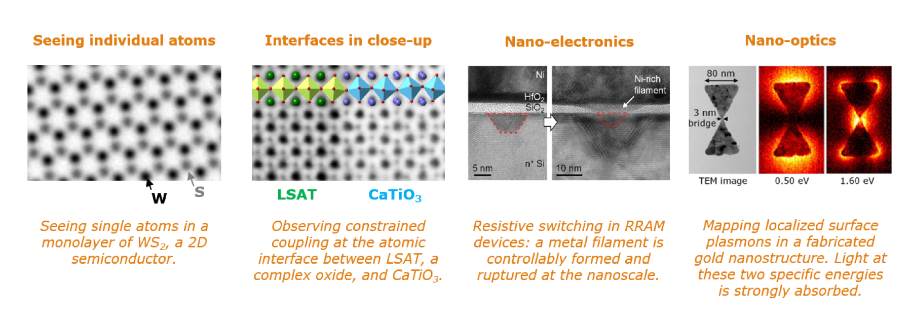
Being able to observe materials directly at atomic resolution allows us to measure new materials properties at surfaces and interfaces. For example: individual dopants and vacancies in 2D materials can be imaged. It is also possible to study microelectronic logic- or memory devices at the ultimate resolution, with the help of careful, site-specific sample preparation.
Our Instruments
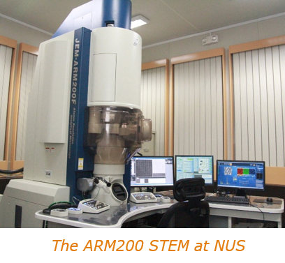
- JEOL ARM200CFEG STEM with ASCOR aberration corrector,
- Quantum ER EELS detector and Oxford X-Max EDS detector
- DENSsolutions Lightning in-situ heating and biasing sample holder
- Quantum Detectors Medipix3 MerlinEM S pixelated detector
- FEI Versa 3D Focused Ion Beam (FIB)
- Gatan Disc Grinder for sample preparation
- Tools for sample handpolishing
- Leica Ion Milling system
- UHV baking chamber
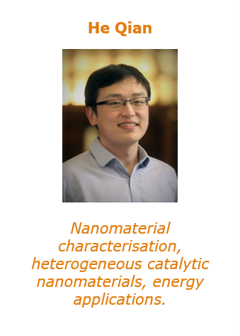
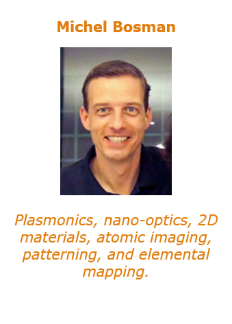
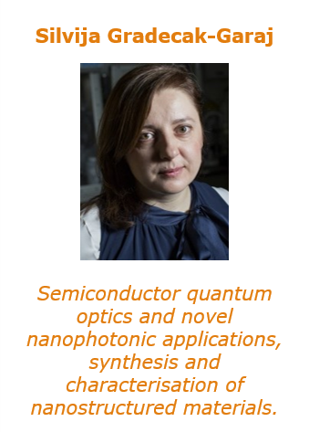
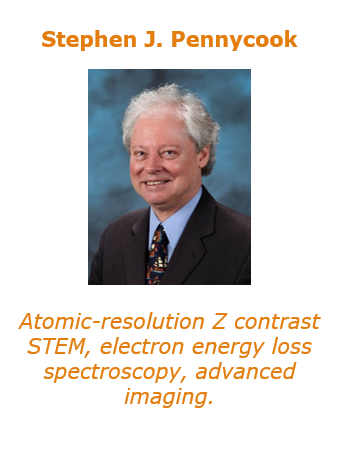
Principle Investigators