
NUS and Applied Materials have announced a major expansion of their joint semiconductor research lab, co-hosted by CDE and the Faculty of Science, aimed at enhancing Singapore’s position as a hub for advanced semiconductor technology.
A launch ceremony marking the expansion of the Applied Materials-NUS Advanced Materials Corporate Lab was held at NUS on 24 October 2024, with Mr Heng Swee Keat, Deputy Prime Minister and Chairman of the National Research Foundation as Guest-of-Honour alongside industry leaders, government officials and senior members of the university.
In his address, Mr Heng touched on the importance of semiconductors and their role in our lives. “In an increasingly digital and digitalised world, semiconductors are essential to powering and enabling our daily lives – at home, at work, and in essential services like healthcare and transport,” he said. “The concurrent green transition, to build a more sustainable future, will demand even more innovations in semiconductors.”
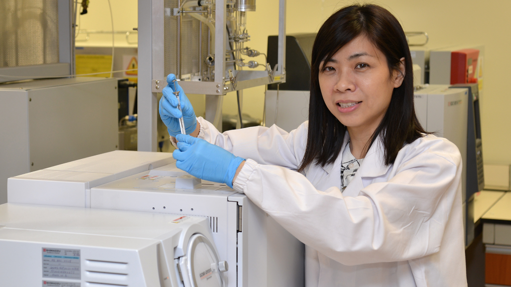
Located at NUS’s Kent Ridge campus, the Phase II expansion of the lab will provide cutting-edge facilities to drive the discovery and development of new semiconductor technologies. Originally established in 2018 and supported by the National Research Foundation (NRF) under the Research, Innovation and Enterprise 2025 (RIE2025) plan, the expanded lab will include a state-of-the-art cleanroom with new semiconductor processing equipment.
Speaking at the launch ceremony, NUS President Professor Tan Eng Chye highlighted the success of the collaboration so far. “The Corporate Lab has made significant strides, with several innovations progressing from the research stage to the scale-up phase. This transition is vital, as it paves the way for real-world applications and benefits,” he said. “This solid partnership between Applied Materials and NUS, and the strong foundation we have built through the Corporate Lab have given us the confidence and fortitude to expand our collaboration into Phase II.”
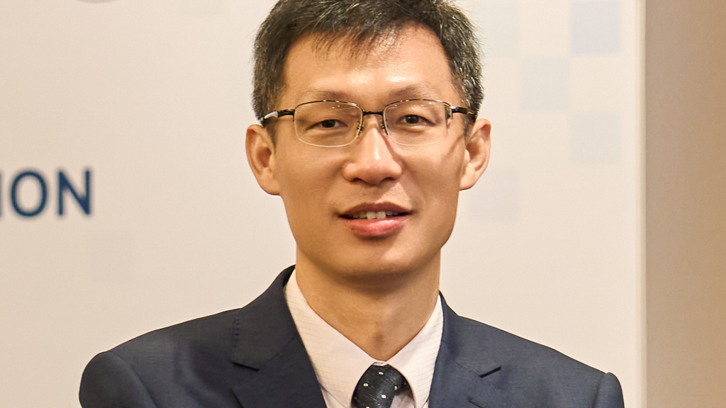
Dr Satheesh Kuppurao, Group Vice President of Business Development and Growth for Applied Materials’ Semiconductor Products Group, emphasised the lab’s importance in fostering industry-academia partnerships. “Our joint work has resulted in numerous patents related to chemistry, semiconductor process and hardware design solutions, along with sponsoring several scholarships,” he said. “Applied Materials is excited to build on our success with NUS and bring enhanced semiconductor research and talent development opportunities to Singapore.”

The upgraded lab will focus on integrated semiconductor processes and interface engineering, accelerating the process of transitioning innovations into commercial applications. By offering enhanced research capabilities and interdisciplinary collaboration, the lab will address complex challenges in semiconductor manufacturing.

The expansion will also see the introduction of the Applied Materials Professorship at NUS, aimed at attracting top international scientists and engineers to conduct research and mentor the next generation of talent in Singapore. Commenting on the new professorship in his speech, Mr Heng said: “Through this Professorship, NUS can bring in top-tier global talent to pursue research and also groom next-generation semiconductor talent.” He added, “It is commendable that Applied Materials and NUS will work together to co-develop new educational and training programmes, including a Masters in Semiconductor Technology and Operations. This will support the development of a broader pool of specialist talent.”