From smartphones to the most advanced AI processors, every technological leap has been built on the art of making things smaller; cramming more processing power into an ever shrinking space.
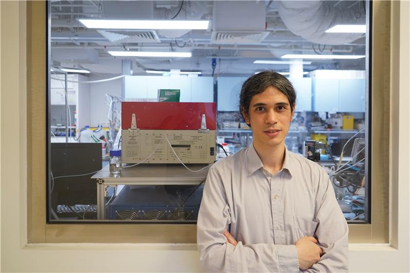
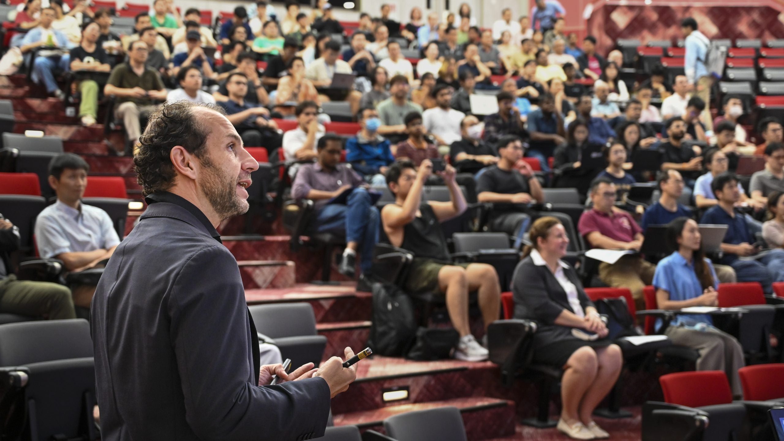
But as Professor Erwin Kessels from the Department of Applied Physics at Eindhoven University of Technology and the current Applied Materials Visiting Chair Professor at NUS told an audience at CDE, technology has now reached the point where smaller isn’t enough.
“Precision at the atomic level is the new frontier,” he said.
Prof Kessels was delivering a public lecture titled “Well Mr Feynman, There Is No More Plenty of Room at the Bottom: Atomic-Scale Processing for Future Chips and Beyond.”
The title referenced Nobel physicist Richard Feynman’s famous 1959 Caltech lecture “There’s Plenty of Room at the Bottom,” in which he imagined a future where scientists could manipulate matter atom by atom.
Decades before such precision was technologically possible, Feynman’s ideas laid the conceptual foundation for a field that is now known as nanotechnology. It was also instrumental in shaping the semiconductor industry’s relentless drive toward miniaturisation.
That process was famously captured in Moore’s Law, the observation proposed in 1965 by Gordon Moore, co-founder of Intel, that the number of transistors on a chip doubles roughly every two years.
“For more than six decades, Moore’s Law has guided chip innovation,” said Prof Kessels. “But now, the ‘plenty of room’ Feynman spoke about has almost been used up.”
Atomic-scale processing
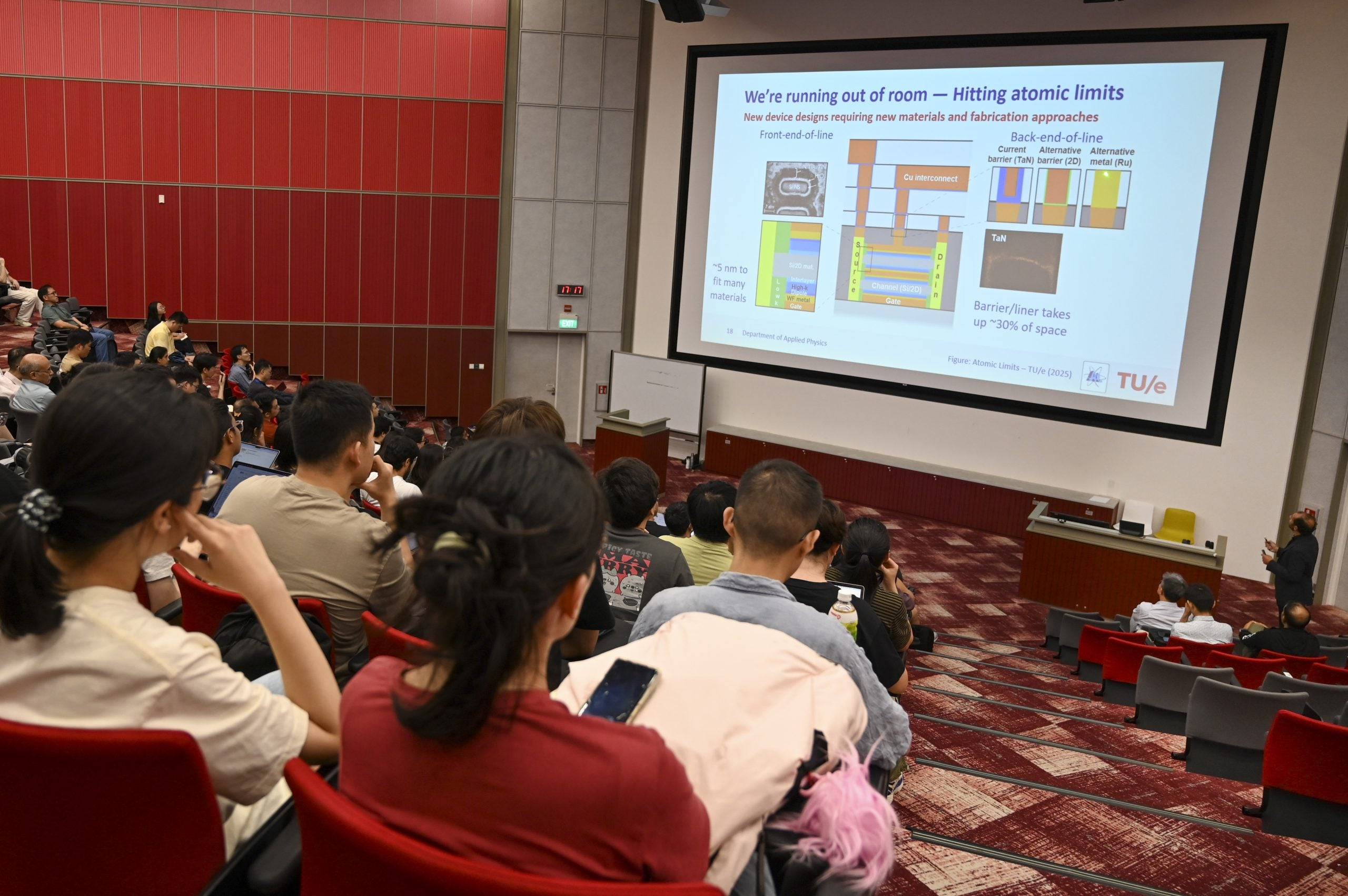
Speaking to an audience of around 200 students, researchers and other guests, he explained how transistors have shrunk to the scale of just a few nanometres, driving the industry into the “Angstrom era”, where even the tiniest structural features demand new materials and techniques.
“We are now in the era of atomic-scale processing,” he said, “where the vision Feynman described more than 60 years ago is finally being realised.”
Among his many roles, Prof Kessels also heads the AtomicLimits blog, an online platform that bridges research and industry perspectives in atomic-scale processing. Through this initiative, he encourages exploration of new frontiers through intelligence, collaboration, and creativity, extending Feynman’s spirit of curiosity into the modern era of atomic precision.
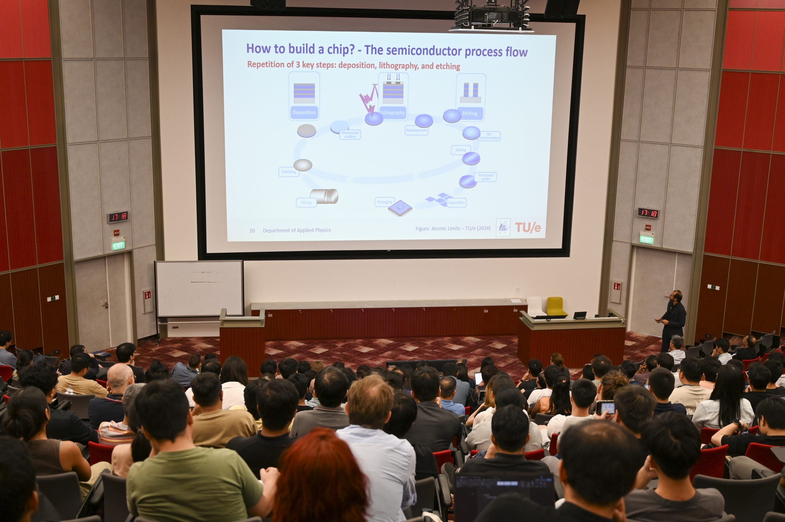
In the lecture, Prof Kessels outlined how extreme ultraviolet (EUV) lithography, one of the most complex manufacturing technologies ever developed, now enables chipmakers to define features at the smallest possible scales. The technology relies on a process so intricate, he said, that the resulting lithography machines are the most complex mechanical systems on Earth.
“These tools are crazy, what they can do,” he told the audience.
Three-dimensional architectures
Complementing these advances are methods known as atomic layer deposition (ALD) and atomic layer etching (ALE) that add or remove material one atomic layer at a time. These provide the control needed to build highly intricate three-dimensional architectures for next-generation logic and memory chips.
ALD and ALE techniques are the core technologies used to develop the next generation of materials for the semiconductor industry under the Applied Materials-NUS Advanced Materials Corporate Lab.
Among the latest emerging techniques, Prof Kessels pointed to the growing importance of area-selective ALD which enables materials to form only where they are needed. By chemically controlling surfaces to encourage or block growth, this “bottom-up” approach could reduce reliance on complex lithography steps, cut manufacturing costs, and further improve precision at the nanoscale.
“It’s about growing material with atomic precision only at the right place,” Prof Kessels said, presenting an engaging short video using LEGO bricks to help visualise the technique.
While atomic-scale processing has become essential to semiconductor fabrication, he also pointed to the growing use of ALD and ALE in other fields such as solar cell design and materials for new generations of batteries. “We’re seeing the same principles that transformed microelectronics being applied to energy conversion, storage, and even emerging quantum systems,” Prof Kessels said.
In other recent developments, Prof Kessels highlighted the move toward AI-driven materials discovery, where machine learning could accelerate the development of new fabrication processes, integrating AI with atomic-scale processing workflows. “Intelligent design will help us discover new materials and optimise how we make them,” he said.
Concluding his lecture, Prof Kessels reflected on the enduring influence of Feynman’s ideas.
“Although we are running out of physical room at the bottom, there is still plenty of room at the intelligent scale, as we keep developing ingenious ways of making things.”
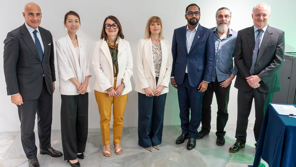
Held on October 15, 2025, Prof Kessels’ lecture was part of the Applied Materials (AMAT) Visiting Chair Professorship at NUS. The professorship brings global academic leaders to the AMAT-NUS Advanced Materials Corporate Lab, hosted at CDE, to collaborate and connect with experts across Singapore's semiconductor ecosystem.

