System Overview
- Process viewing Cut & See

- Failure analysis
Technical Specifications
- Up to 8” wafer inspection in both SESM as in FIB operation enable by the new triple lens design
- Max Specimen Height: 96 mm (with rotation stage); 137 mm (without rotation stage)
- Integrated TOF-SIMS with a compact TOFSIMS dector and uses FIB column as primary ion beam with 3D compositional analysis
- Magnification at 30kV: 4x-1,000,000x
- Maximum Field of View: 4.3 mm at WD; analytical 5 mm; 7.5 mm at WD 30mm
- Electron Beam Energy: 200 eV to 30 keV down to 50eV with Beam Deceleration mode
- FIB Resolution : <2.5nm at 30kV (at SEM-FIB coincidence point)
- Accelerating voltage: 0.5 kV to 30 kV
- Ion Gun : Ga Liquid Metal Ion Source
- Probe Current: 1 pA to 50 nA
- FIB angle: 55 degree
- Gas injection system : Tungsten and Platinum
- Model: TESCAN GAIA3
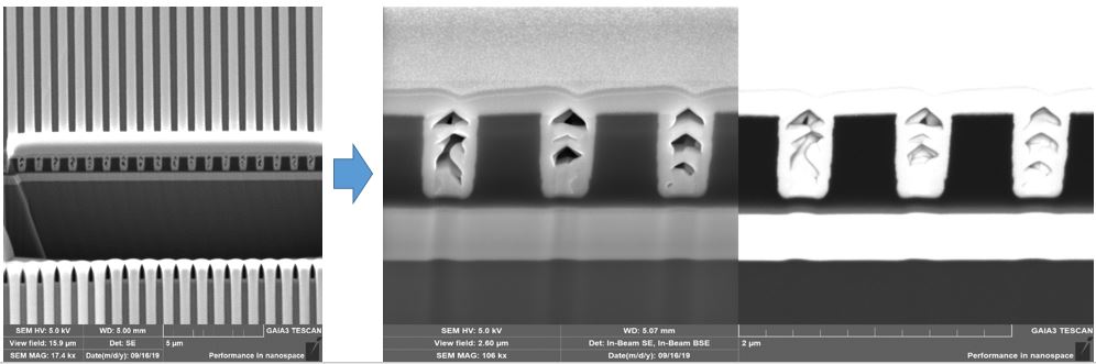
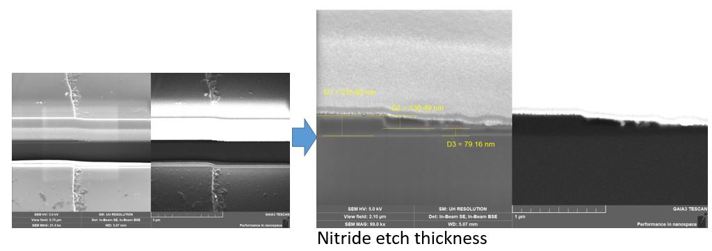
Quality of Patterned Resist

Location: E6-03-02, Metrology
Contact: e6nanofab@nus.edu.sg