LASER MICRO-MACHINING SERVICE

Overview

Custom Laser micro-machine system operating on a femtosecond pulsed laser. The short pulse length limits local heating effects reducing Heat Affected Zone (HAZ). Applicable in wide range of materials. Especially effective for ceramics, metals and selected Polymers.

• Ceramics* : Alumina oxide, Aluminium nitride, etc
• Wafers*     : Silicon, Silicon Nitride, Silica (Glass), etc
• Polymers   : Polyamide, Kapton, PMMA etc.
• Metals*     : Stainless Steel, Copper, Aluminium etc.

We routinely perform and achieve the following precision:
1. 15 micron Percussion holes on ceramics, thin metals and silicon wafers with precision of <1 micron for ceramics.
2.  30 micron minimum Circular holes on ceramics, thin metals and silicon wafers with highest precision of <1micron for 
     ceramics.
3.  Smallest feature size > 20 microns with precision 1 micron on metal sheets, ceramics and polymers.
4.  Dicing of Silicon wafer up to 750um thick with negligible dust on surface.

Remarks: Subjected to maximum material thickness between 500um ~ 700um* 


  1.   Ceramic Material

          Electrodes for ion trapping: We provide blade electrodes for 3D ion traps based on ceramic materials. These are used
          for quantum information processing and atomic clock projects.

            Laser Micro-machining_Ceramics Materials                    50um slot milling on 250um thickness Alumina oxide

    2.   Polymer Material

          Custom etching of heat sensitive Polymer material of approximately 50um thickness with features between 50um to
          100um width.

          Sample: Consistent output of 50um Polymer strip with 50um thickness material.


    3. Metals Material

    Sample A: Sepertine metal feature, 25um width trip   
    on a 50um thickness stainless Steel

L3 Laser Micro-machining_Metals Materials (Demo)

Sample B: Micro laser etching on 1 mm Titanium tube

L3 Laser Micro-machining_1mm Titanium Tube (Demo)

4. Silicone Material

      Sample A: Custom dicing of 535um thickness
      silicon wafer with circuits

L3-Laser-Micro-machining_Custom-dicing_525um-thick-silicon-wafer-w-circuits-1536x1154

Sample B: Custom shape dicing of silicon wafer of 525um thickness

    5.  Graphene Material

      Precision percussion holes on thin Graphene sheet.          

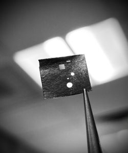
   Sample: Precision percussion holes on thin Graphene sheet.

   For quotation, please send your request to the person in charge stating your sample feature sizes, tolerances, volume,
   and materials.

  Tel:  6516 8549

  Email:  tonywong@nus.edu.sg

  In Charge:  Mr. Tony Wong