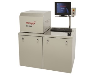
The NanoNex 2000 Imprint System delivers both thermal and UV nanoimprint lithography for advanced micro- and nanopatterning. Engineered for optimal performance on ceramic sol-gel surfaces, the system features built-in capabilities for extending master mold lifetime through intermediate polymer and ceramic sol-gel stamp replication processes. Additional technical specifications are outlined below.)
Technical Specifications
• Exposure Optics: UV400 broadband; I-line (365 nm) and G-line (405–436 nm) • Lamp Power: ~350 W Hg lamp • Exposure Modes: Proximity, soft/hard contact, low-vacuum & vacuum contact, flood exposure • Top-Side Alignment (TSA) with X/Y/Θ micro-positioning; accuracy ~±0.5 µm • Manual X/Y/Θ micro-positioning with microscope viewing for small areas • Proximity Gap: Programmable ~10–300 µm (1 µm steps, tool-dependent) • Substrate Size: Irregular chips/dies up to 2″ wafers (< 4mm thick) • The max coupon size is 2cm square • Mask Size: Typically 3″ square chrome/glass masks (user-supplied) • Vacuum contact: ~0.4–0.6 µm • Soft-/hard-contact: ~0.5–1 µm • Proximity (~20 µm gap): ~2.5–3.5 µm