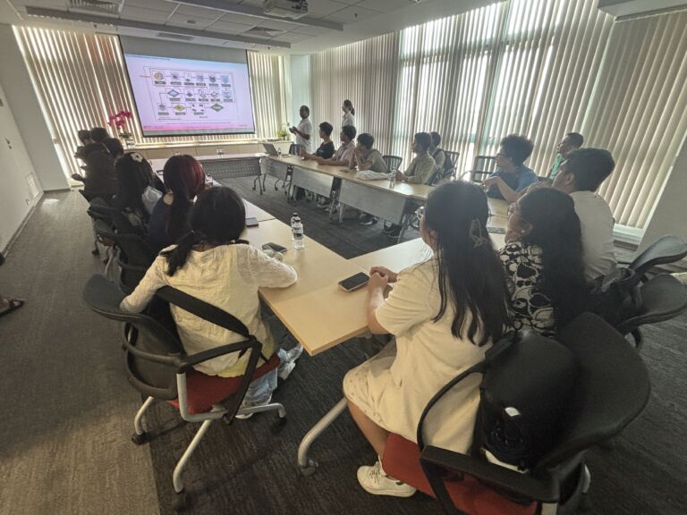
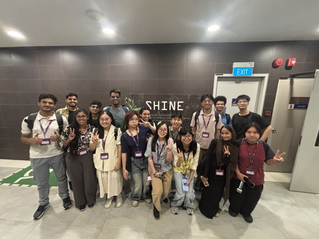
On 25 June 2026, E6NanoFab welcomed 18 students from the 2026 NUS Young Fellowship Programme for a visit to our advanced nanofabrication and microelectronics facilities.
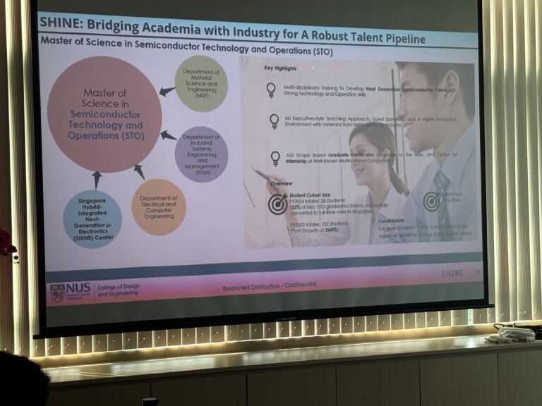
The visit began with an introduction by Dr Manohar Lal, who provided an overview of E6NanoFab’s research capabilities and infrastructure. Students were also introduced to the Master of Science in Semiconductor Technology and Operations (MSc STO) programme offered by the NUS College of Design and Engineering, launched in 2024, which now features a specialisation in Applied AI for Materials and Process Engineering.
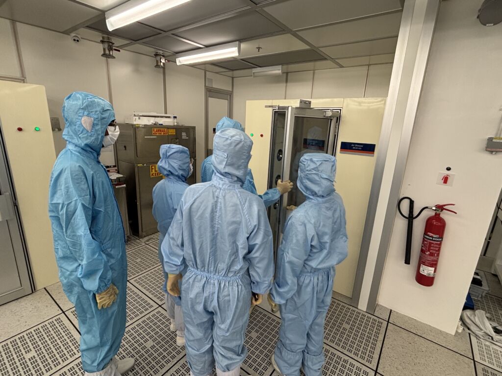
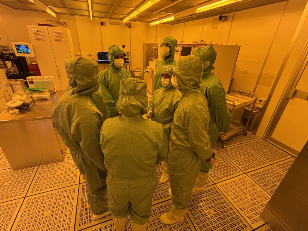
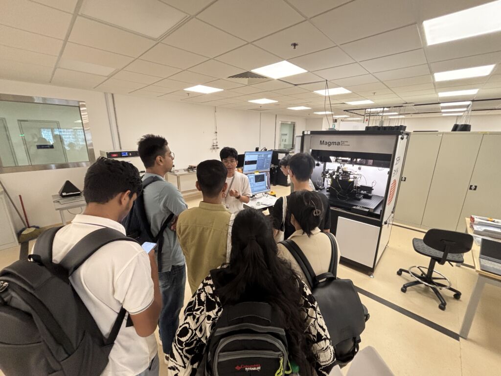
Students then toured E6NanoFab’s cleanroom and laboratory facilities, gaining exposure to key processes including deposition, lithography, metrology, characterisation, and advanced packaging. The tour also included the Advanced Packaging Lab at the SHINE Centre, offering a broader view of the semiconductor manufacturing ecosystem.
Through this visit, students gained insights into advanced semiconductor technologies, research environments, and postgraduate pathways at NUS. The experience aimed to encourage interest in science, engineering, and innovation-driven careers.
E6NanoFab thanks our researchers, engineers, laboratory officers, and the SHINE Centre team for their support in making the visit a success.