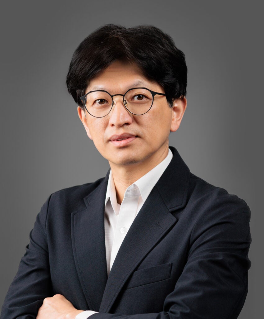
Education
D.Phil of Condensed Matter Physics, Oxford University (UK) / 2006
Experience
- Process Engineer / TSMC (Taiwan) / Oct 1997 – Jul 1999
- Senior R & D Engineer, TSMC (Taiwan) / Jul 1999 – Jun 2002
- *Assistant Professor, School of Materials Science and Engineering, Nanyang Technological University (Singapore) / Jun 2006 – Dec 2009
- *Associate Professor, Academia Sinica (Taiwan) / Feb 2010 – Apr 2014
- *Full Professor (Tenured), Institute of Atomic and Molecular Sciences, Academia Sinica (Taiwan) / May 2014 – Jul 2014
- *Associate Professor, King Abdullah University of Science and Technology (Saudi Arabia) / Aug 2014 – Jul 2016
- *Full Professor, King Abdullah University of Science and Technology (Saudi Arabia) / Aug 2016 – Dec 2017
- *Director, Corporate Research in Taiwan Semiconductor Manufacturing Company (Taiwan)/Dec2017-present
- *Mar 2021-Nov 2024, Chair Professor at University of Hong Kong
Research Interests
Lance Li’s group is focusing on the growth of large-area high-quality 2D semiconductors and the development of advanced device technologies, such as metal contact, dielectrics scaling, and new architecture, for advanced semiconductor nodes to continue the scaling of transistors. This group is also exploring energy efficient devices beyond Si technologies.
Selected Publications
- Y.C. Lu et al. Projected performance of Si- and 2D-material-based SRAM circuits ranging from 16 nm to 1 nm technology nodes. Nature Nano. (2024) 19, 1066 – 1072.
- J. Shen et al. Engineering grain boundaries in monolayer molybdenum disulfide for efficient water/ion separation. Science (Accepted)
- J.H. Fu et al. Oriented lateral growth of two-dimensional materials on c-plane sapphire. Nature Nano.(2023) 10.1038/s41565-023-01445-9.
- J.K. Huang et al. High-κ perovskite membranes as insulators for two-dimensional transistors, Nature(2022) 605 (7909), 262-267.
- Y. Wan et al. Low-defect-density WS2 by hydroxide vapor phase deposition., Nature Comm. (2022) DOI 10.1038/s41467-022-31886-0
- P.J. Shen et al. Ultralow contact resistance between semimetal and monolayer semiconductors, Nature(2021) 593 (7858), 211-217.
- T.-A. Chen et al. Wafer-scale single-crystal hexagonal boron nitride monolayers on Cu (111), Nature(2020) 579, 219–223.
- A.Y. Lu et al. Janus monolayers of transition metal dichalcogenides. Nature Nano. (2017) 12(8), 744-749
- M.Y. Li et al. Epitaxial growth of a monolayer Wse2- MoS2 lateral p-n junction with an atomically sharp interface.Science (2015) 349(6247), 524-528.
- M.H. Chiu et al. Determination of band alignment in the single-layer MoS2-WSe2 heterojunction. Nature Comm. (2015) doi:10.1038/ncomms8666
- Lee, Y. H. et al. Synthesis of large-area MoS2 atomic layers with chemical vapor deposition. Advanced Materials (2012) 4(17), 2320-2325.


