


The global semiconductor market is approaching US$1 trillion in annual sales, driven by growing demand for faster computers, smarter AI systems and more powerful electronic devices. Singapore, which produces one in 10 of the world’s chips, has a direct stake in sustaining that trajectory. For decades, advances in chip performance have relied on shrinking transistor size, pushing semiconductor technology ever closer to its physical limits. But a bottleneck is emerging at one of the most fundamental levels of chip architecture: the tiny wiring inside computer chips. While the copper wires connecting transistors are becoming smaller with each new generation, the protective layers around them cannot shrink as easily, making it harder to improve chip speed, efficiency and reliability.
Copper wires inside chips need two protective coatings: a barrier to stop copper atoms from migrating into surrounding materials, which can cause short circuits and chip failure, and a liner to help copper adhere and form smooth, reliable connections. Today’s standard coatings, made from tantalum-based materials, must be at least four nanometres thick to function. In the next generation of chips, these protective layers could take up as much as half of the wire’s cross-section, sharply increasing electrical resistance and reducing chip speed and efficiency. A collaboration between the National University of Singapore (NUS) and Applied Materials has now resulted in a single material thin enough to preserve copper’s share of the wire yet capable of performing both of these functions.
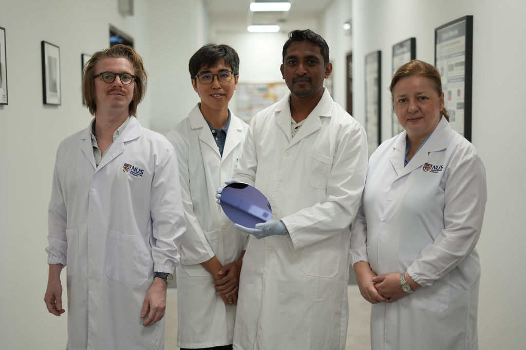
Researchers at the Applied Materials–NUS Advanced Materials Corporate Lab, working across the Department of Materials Science and Engineering in the College of Design and Engineering at NUS (NUS CDE) and the Department of Chemistry at the NUS Faculty of Science, together with researchers from Applied Materials, developed a process for growing crystalline tungsten disulfide (WS2) films just 0.7 nanometres thick — roughly the width of a few atoms — on industry-standard 200-millimetre wafers. Published in Nature Electronics on 31 March 2026, the study shows that even an atomically thin WS₂ monolayer can serve as both barrier and liner, allowing chipmakers to keep shrinking circuits without sacrificing speed or reliability.
“Importantly, the process works at low temperatures and across full wafers, making it readily compatible with existing chip manufacturing lines”, stated Dr M. Juvaid Mangattuchali, who had co-led the research with Dr Hippolyte Astier, both from the Department of Materials Science and Engineering.

One layer, two functions
The researchers first demonstrated that as a liner, the WS2 coating helps copper form a smooth, continuous film rather than forming disconnected clusters — a problem that affects ultrathin copper deposited directly on a chip’s insulating layer. With coating, the resistance dropped by more than a millionfold compared with uncoated surfaces. The single atomic layer also outperformed the conventional tantalum-based stack by roughly five times, despite being nearly 10 times thinner — 0.7 nanometres vs approximately six nanometres for the industry standard.
The thickness gap has direct implications for chip performance. In a future 20-nanometre-wide wire, the current industry coating would occupy 40 per cent of the wire’s diameter. The WS2 layer takes up just 7per cent, leaving substantially more room for copper to carry current.
The team then investigated whether the same ultrathin WS2 layer could also serve as a barrier to stop copper atoms from leaking into surrounding chip materials. Under prolonged heat stress, copper on uncoated surfaces reacted with the underlying silicon, forming large defective structures. With a single WS2 layer in place, no reaction or intermixing occurred. Moreover, under electrical stress, the WS2 barrier extended projected wire lifetimes by more than 10-fold compared with unprotected devices.
“The key challenge was ensuring that a layer so thin could still function reliably as both a liner and a barrier. Conventional wisdom held that you needed two separate materials — one for the barrier, one for the liner — with a combined thickness of at least four nanometres. Showing that a single monolayer of WS2 can do what that two-layer stack currently does opens the door to a fundamentally different approach to interconnect design,” said Professor Silvija Gradečak from the NUS Department of Materials Science and Engineering, and Co-Director of the Corporate Lab.
Computational modelling by researchers in NUS’ Department of Chemistry revealed why the material’s structure makes it particularly effective as a barrier. The WS2 grown by this process is composed of many tiny crystalline grains, and in multilayer films those grains are randomly oriented from one layer to the next. Defects and grain boundaries therefore do not align across layers — much like offset joints in a brick wall — making it substantially harder for copper atoms to pass through.
“The calculations showed us that the polycrystalline nature of these films, which might initially seem like a limitation compared with a perfect single crystal, is actually an asset. The random grain orientations between layers create a labyrinth that copper atoms struggle to traverse,” said Professor Richard Wong from the NUS Department of Chemistry, who is also a Co-Director of the Corporate Lab. “This gives us a design principle, where we engineer the grain structure to optimise barrier performance instead of pursuing perfect crystallinity.”
Designed for the production line
For any new material to enter chip manufacturing, it must meet strict production requirements. The team’s growth process — thermal atomic layer deposition at 350 degrees Celsius, without plasma — satisfies all four key requirements for integration into existing chip fabrication lines: a temperature low enough to avoid damaging underlying chip layers; uniform coverage across an entire industry-standard wafer; precise thickness control down to a single atomic layer; and conformal coating of deep, narrow trenches (greater than 95 per cent coverage at depth-to-width ratios of 10 to 1). No previous method for growing two-dimensional materials had met all four simultaneously.
“The resulting films are thinner than any barrier or liner target on the international semiconductor technology roadmap through to 2037, positioning the material not just for the next generation of chips but potentially for several generations beyond,” said Dr Astier.
“Many promising materials are being explored, but the gap between a research demonstration and a process that can run in a production facility is substantial. By working through the Corporate Lab, we were able to test these films against the constraints that chipmakers actually face. Meeting these four requirements with a single continuous film makes this result relevant to the industry,” added Dr John Sudijono, Director of Engineering at Applied Materials, and Co-Director of the Corporate Lab.
Future directions include investigating the 2D interface at the microscopic level to understand how grain structure relates to long-term wire reliability, as well as exploring whether greater control over grain orientation could further improve performance. The study also demonstrates the viability of using the same low-temperature and industry-compatible growth approach to integrate ultrathin 2D materials into other components of future computer chips.