Structural Characterisation
Providing a wide range of tool, training and expertise for Topographic imaging structural characterisation of nanoscale materials.
Structural Charactierisation Facilities
The facility is well equipped with various state-of-art facilities for Nano-Fabrication, Topographic imaging and structural characterization such as Helium Ion Microscope (Orion Nano-Fab), AFM/SPM, Raman spectrometer, Direct laser writer, mask aligner etc. The various facilities are supported by postdoctoral fellows and PhD students who are superusers for specific equipments and manage the facility along with their research work. These include:
- High resolution helium ion microscope is equipped with SE2 detector, charge neutralizer and plasma cleaner to handle a broad range of specimens.
- The focused helium ion beam with sub-nm probe size enables users to write sub-10nm structures by direct milling.
- The Neon ion beam is used to create the desired patterns by fast milling.
- The electron flood gun enables to image insulating samples without any conductive coating which is very essential for biological/insulating specimens.
- Direct laser writer along with Orion Nano-Fab enables to cutting-edging device fabrications.
The labs for respective equipments are well designed to avoid any external disturbances such as acoustics, vibration, air flow, temperature, light etc. room/low temperature Raman along with PL enables us to probe structural fingerprints of the specimens:
How to Access Facilities
To access the facility, the following steps must be followed:
Contact Ngee Hong Teo (mtnh@nus.edu.sg) and Tiho (tiho@nus.edu.sg) to schedule a project meeting.
Register your personal and project details with PPMS (https://ppms.asia/nus-cde/login/)
Schedule a training or service session with our staff.
Service & Booking Fees
Booking fees will differ for NUS and Non-NUS members. More details will be published soon.
Our Partners
Find out more about our partners in Singapore:
Electron Microscopy Facility (EMF)
NUS Center for Bioimaging Sciences (CBIS)
NUS YLL School of Medicine Electron Microscopy Unit (EMU)
NTU Facility for Analysis, Characterization, Testing and Simulation (FACTS)
A*STAR IMRE Advanced Characterization and Instrumentation (ACI) Department
Contact Us
Research Fellow : Tiho@nus.edu.sg
Lab Technologist : Mtnh@nus.edu.sg
Communications : Samuel@nus.edu.sg
T11 Shared Facilities
Level 11
T-Lab Building
5A Engineering Drive 1
College of Design and Engineering
Singapore 117411
FACILITIES
Click on the icon/tab to learn more about our facilities at NUS T11:
Material synthesis
Structural Characterisation
Properties
Devices
Structural Characterisation Facilities
Structural Characterization Tools
Discover more, Click here.
The following are available at our facility: Helium Ion Microscope (HIM), BRUKER XRD, Raman Spectrometer.
Structural Characterization/Morphology
Discover more, Click here.
The facilities consist of Surface Stylus Profiler: Bruker DektakXT, STM-based SPM – JEOL JSPM-5200, Multipurpose Atomic Force Microscope: ParkAFM-NX10.
Structural Characterization Tools
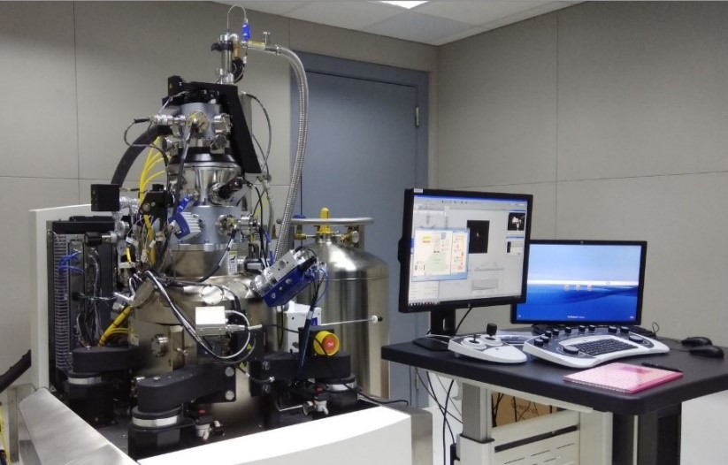
Helium Ion Microscope(HIM)
This state-of-the-art instrument “Orion Nano-Fab” allows both fast machining of sub-10 nm structures and high-resolution surface-sensitive imaging in the same instrument. At the nanoscale, it enables imaging (topography), patterning, lithography, ion irradiation, compositional differences, crystal grains etc. It is equipped with electron flood gun, plasma cleaner and two beam sources Helium and Neon. The electron flood-gun enables easy imaging of insulating samples while plasma cleaner lets to remove the redundant hydrocarbon layers. The Gas field ion source (GFIS) technology & advanced column for ultra-accurate beam focus and smaller sample interaction volume lead it to achieve sub-nanometer resolution.
Technical Specifications:
- Scanning ion microscope
- Source beam: Helium/Neon
- Advanced Nanopatterning software: Nano-Patterning and Virtualization Engine(NPVE)
- ET secondary electron detector
- Electron flood gun for charge compensation
- Motorized 5 axis eucentric stage ( where x, y, z, r are all piezo driven)
- Field of view: 800 μm – 100 nm @ 8 mm working distance.
- Beam diameter: 0.5 nm @30kV; Beam energy: 10 – 30 kV; Beam current: 0.1 to 100 pA ( for Helium ion beam)
- Beam diameter: 1.9 nm @ 25kV; Beam energy: 10 – 25 kV; Beam current: 0.1 to 50 pA (for Neon ion beam)
- Patterning Resolution: ~ 8nm line width @25 kV for Helium and ~20 nm for Neon.
- Pattern generator frequency: 2GHz.
- Plasma cleaner (Evactron) for removing hydrocarbons.
- Stage travel: x = 48 mm, y = 48 mm, z = 8 mm, Rotation: 0 - 360°, Tilt: 0 – 54°
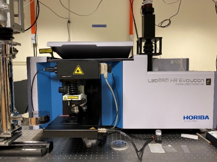
Raman Spectrometer
The LabRAM HR Evolution Raman microscopes are ideally suited for both micro and macro measurements, and offer advanced confocal imaging capabilities in 2D and 3D. The true confocal Raman microscope enables the most detailed images and analyses to be obtained with speed and confidence. With guaranteed high performance and intuitive simplicity, the LabRAM HR Evolution is the ultimate instrument for Raman spectroscopy. They are widely used for standard Raman analysis, PhotoLuminescence (PL), Tip Enhanced Raman Spectroscopy (TERS) and other hybrid methods.
Technical Specifications
- JY Horiba LabRAM Evolution
- Detector range- 550-1050nm, > 70cm-1
- Excitation Laser: 488 nm & 514 nm
- Able to measure both Raman and Photoluminescence
- Spatial mapping of surfaces
- Temperature Range: 10 K – 300 K
- Horiba Jobin Yvon LabRAM | Raman Lab
Surface Characterisation/Morphology
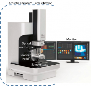
Multipurpose Atomic Force Microscope: ParkAFM-NX10
The Park NX10 AFM features a True Non-Contact™ scan Mode that produces high resolution and accurate data by preventing destructive tip-sample interaction during a scan. Its compact and rigid ‘Step-and-Scan’ enables programmable multiple region imaging.
______________________________________________________________________________________
Technical Specifications
- 2D Flexure-Guided Scanner with XY Scan Range 50 μm x 50 μm
- XY-resolution: 0.05 nm
- Z-Resolution: 015 nm
- Field-of-view: 480 µm × 360 µm (with 10× objective lens)
- Powerful system control and data acquisition software (Park SmartScanTM)
- Auto mode for quick setup and easy imaging
- Stand-alone design of AFM data analysis software ‘XEI’
Incorporated Scanning Modes
- True Non-ContactTM mode
- Intermittent (tapping) mode
- Contact mode
- Phase imaging
- Lateral Force Microscopy (LFM)
- Force-Distance (F/D) Spectroscopy
- Piezoelectric Force Microscopy (PFM)
- Electric Force Microscopy (EFM)
- Kelvin Probe Force Microscopy (KPFM)
- Magnetic Force Microscopy (MFM)
- Conductive AFM (C-AFM)
- QuickStep Scanning Capacitance Microscopy (SCM)
- PinPoint™ Conductive AFM
- Nanoindentation
- Nanolithography
- Force Modulation Microscopy (FMM)
