Devices
Providing a wide range of support for various interdisciplinary research, the Litho Lab & Cleanroom facilities are equipped for UV lithography, thin film coating, reactive ion etching etc.
Thin Film Deposition Facilities
The Litho Lab consists of a clean room fully equipped for UV lithography and other processes (e.g. thin film deposition, RIE/ICP dry etching, etc.):
- Lithography includes laser writing system for mask making and direct writing, and a conventional mask aligner for pattern transfer.
- Thin film deposition includes thermal evaporation (Cu, Au, etc.) and e-beam evaporation (Cr, Ti, Al, etc.)
- Dry etching includes RIE/ICP etching equipment for dry etching of Si, oxide compound and other materials with process gases Ar, CF4, C4F8, CHF3, He, N2, O2, SF6.
The Litho Lab
Providing support for the various and interdisciplinary research, such as Multifunctional (oxide) materials; Ferroelectric tunnelling junction; Superconductor-insulator transitions; Ambipolar superconductivity; Hall effect measurements; Spin pumping; Electric control of magnetism; Plasmonic transducer; Fe2O3-H-doping; Graphene nanochannels; Hybrid integrated flexible electronic, Metamaterials, etc.
Clean room facilities have following facilities to support the various and interdisciplinary research such as a class 10K cleanroom with the following equipment.
- Heidelberg DWL66 laser writer for mask writing and direct writing capabilities;
- MJB4 SUSS Mask aligner;
- CEE Spin coater;
- Hot plates;
- AJA e-gun and thermal evaporator;
- Sentech SI 500 ICP etcher
- Bruker Dektat Contact Profiler;
- Optical microscope (Olympus);
How to Access Facilities
To access the facility, the following steps must be followed:
Contact Ngee Hong Teo (mtnh@nus.edu.sg) and Tiho (tiho@nus.edu.sg) to schedule a project meeting.
Register your personal and project details with PPMS (https://ppms.asia/nus-cde/login/)
Schedule a training or service session with our staff.
Service & Booking Fees
Booking fees will differ for NUS and Non-NUS members. More details will be published soon.
Our Partners
Find out more about our partners in Singapore:
Electron Microscopy Facility (EMF)
NUS Center for Bioimaging Sciences (CBIS)
NUS YLL School of Medicine Electron Microscopy Unit (EMU)
NTU Facility for Analysis, Characterization, Testing and Simulation (FACTS)
A*STAR IMRE Advanced Characterization and Instrumentation (ACI) Department
Contact Us
Research Fellow : Tiho@nus.edu.sg
Lab Technologist : Mtnh@nus.edu.sg
Communications : Samuel@nus.edu.sg
T11 Shared Facilities
Level 11
T-Lab Building
5A Engineering Drive 1
College of Design and Engineering
Singapore 117411
FACILITIES
Click on the icon/tab to learn more about our facilities at NUS T11:
Material synthesis
Structural Characterisation
Properties
Devices
Lithography
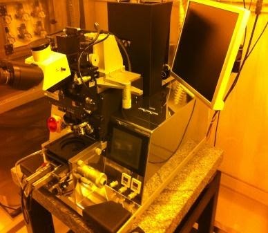
Mask aligner: SUSS Microtec- MJB4
The mask aligner is a faster way to write the pattern using pre-written mask. It operates in either contact or proximity mode.
Technical Specifications:
Minimum substrate size: 5x5 mm2
Mask size: 6”x6”
Source: DC lamp (405 nm)
Source power: 70 mW
Resolution: 3 um
Location: T-Lab, level 11, Clean Room and Litho-Lab
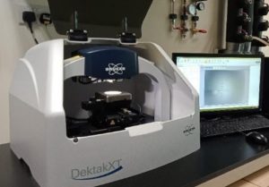
Surface Stylus Profiler: Bruker DektakXT
The profiler is a fast and easy-to-use counterpart of atomic force microscope. It is very reliable for measuring step height of 50nm to >1um.
Technical Specifications
- X and Y Stage: 2µm repeatability.
- Z Stage: Soft touch stylus null.
- Fast data collection and analysis.
Location: T-Lab, level 11, Litho Lab
Spin Coater: Cee® 200X
Fully programmable and user-friendly, the Cee® 200X features the accuracy and repeatability needed to eliminate processing variability from photoresist and thin film deposition processes
Technical Specifications
- Minimum substrate size: 3x3 mm2
- Maximum substrate size: 8”x8”
- Maximum Speed: 6000 RPM
- Available resists: AZ5214E, AZ9264 & SU-8 resist
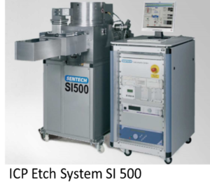
Inductively coupled Plasma Etch system: Sentech-SI500
The SI 500 represents the leading edge for inductive coupled plasma (ICP) processing. It is based on the ICP plasma source PTSA, dynamic temperature controlled substrate electrode, fully controlled vacuum system, advanced SENTECH control software using remote field bus technology, and a very user-friendly general user interface for operating the SI 500.
- Flexibility and modularity are design characteristics of the SI 500 High etch rate; Low damage;
- High aspect ratio; superior homogeneity; User-friendly GUI operational software.
- Available etchants: Standard gas line and MFC with gases (SF6, Ar, O2, N2, C4F8, CHF3) films.
Technical Specifications
Substrate: 100 mm wafer size
Chamber (AlMg) with Liner RF generator
Automatic single wafer vacuum load-lock
RF generator (RIE) /Substrate electrode: power 600 W; frequency 13.56 MHz
RF generator (ICP)/Upper electrode: power 2500 W; frequency 13.56 MHz
Location: T-Lab, level 11, Litho-Lab
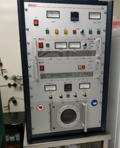
Plasma Etch system: Diener Electronic – PICO 300
Cleaning of surfaces (e.g. before bonding, soldering or gluing)
Activation of surfaces (e.g. before printing, varnishing or gluing)
Available gases: Ar, O2, N2
Technical Specifications
Power: 0-300w
Ar: 0-20sccm; O2: 0-50sccm
Location: T-Lab, level 11, Clean Room and Litho-Lab
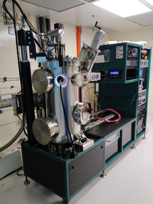
E-beam/Thermal Evaporator: AJA international-ATC-ORION-8E U
This UHV deposition system is capable of producing good quality thin films of metals, alloys and their multilayers. Able to handle 8” wafers size.
Targets:
- E-beam: Ti, Cr, Al
- Thermal: Au, Cu
Technical Specifications
- Load lock best vacuum: 10-7 torr
- Main chamber best vacuum: 10-9 torr
- Cylindrical chamber size: 36″ high x 24″ diameter
- Substrate rotation during deposition
- Equipped with quartz thickness monitor
- Four thermal evaporation sources (molybdenum boats) and 5 E-beam crucible sources (graphite)
Location: T-Lab, level 11, Litho-Lab
