

As transistors inside microchips continue to shrink, the metal wiring that connects them is becoming a growing obstacle to faster, more energy-efficient chips. Narrower wires have greater electrical resistance, while smaller gaps between them increase interference between adjacent signals. These effects impede data transfer and raise energy consumption — an issue known as interconnect bottleneck, which is especially acute in data-hungry artificial-intelligence processors.
A team from the National University of Singapore (NUS) led by Professor Barbaros Oezyilmaz from the Department of Materials Science and Engineering at the College of Design and Engineering, who also holds a joint appointment in the Department of Physics at the Faculty of Science, has developed an atom-thin film of amorphous carbon that could help ease this bottleneck. The film maintained a dielectric constant, or k-value, of 1.35 at thicknesses down to just 0.8 nanometres. It also withstood strong electric fields and prevented copper ions from passing through it.
“This is a more-than-20-year-old materials bottleneck: while transistor technology has changed radically, the basic copper-interconnect platform has remained largely intact and is now one of the dominant obstacles to converting further scaling into real performance and energy gains,” said Prof Oezyilmaz.
Current chip designs use separate materials to insulate copper wires and keep the copper from spreading into the surrounding insulation. Combining both functions in one film could leave more room for wider copper lines, which have lower resistance and could help move data faster while consuming less energy.
The findings were published in Nature Electronics on 18 August 2026.
Calming the nervous system of microchips
Just as networks of neurons carry biological signals between different regions of the brain, interconnects, microscopic wires mostly made from copper, allow data to travel between various parts of a chip.
To limit interference between those closely packed signal paths, each copper wire is separated from its neighbours by an insulating material called a dielectric. Its k-value measures how strongly it responds to an electric field. Lower values reduce unwanted interaction between neighbouring signals. Industry roadmaps have called for a k-value below 2 as the gaps between interconnects shrink below 10 nanometres.
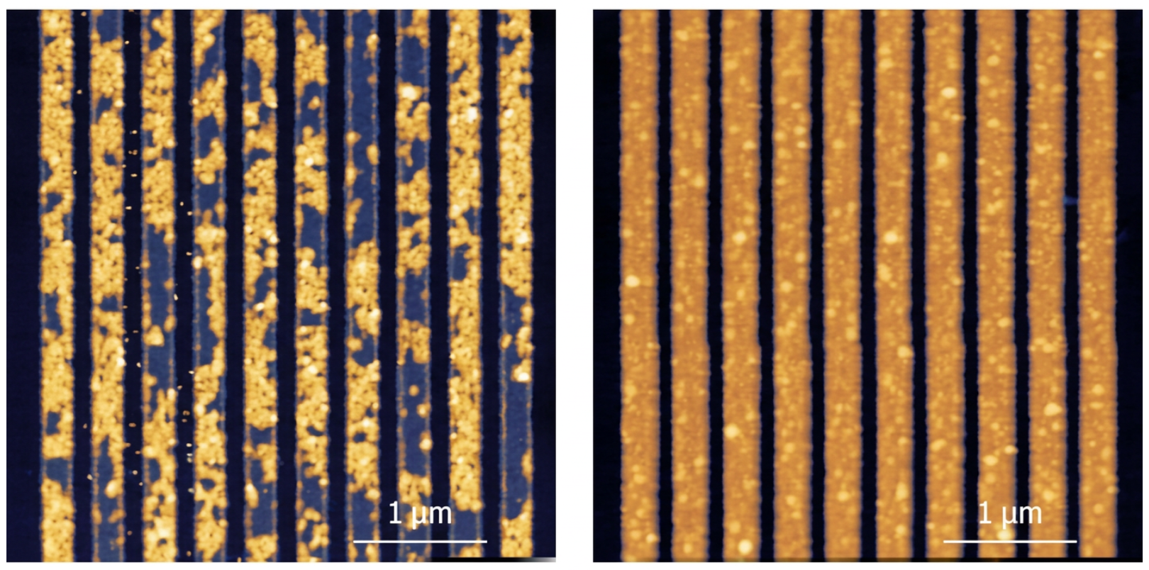
Many low-k materials contain pores that reduce their k-value but also weaken them, making very thin films challenging to produce. On the other hand, denser materials are stronger but tend to have k-value. The NUS team’s carbon film is amorphous, meaning its atoms have no regular, repeating arrangement. Its k-value remained close to 1.35 across thicknesses from 0.8 to 2.7 nanometres, staying well below the industry target even when less than one nanometre thick.
“Carbon can conduct electricity in many forms, so at first it may seem an unlikely choice for an insulator,” said co-first-author Dr Toh Chee Tat from the Department of Materials Science and Engineering at NUS CDE and the NUS Centre for Advanced 2D Materials (CA2DM). “In our film, the atoms are arranged randomly. This disorder restricts how freely the electrons can respond to an electric field, allowing the k-value to remain low even when the film is extremely thin.”
Two birds with one stone
A low k-value addresses only one part of the problem. Over time, copper can migrate from a wire into the surrounding insulation, where it can form unintended electrical paths and eventually cause the device to fail. Chipmakers therefore add a separate barrier layer, often made from tantalum nitride, to keep the copper in place. This barrier takes up some of the limited space available for the wire itself.
In accelerated tests, a carbon film just 0.8 nanometres thick prevented copper from passing through it. Its projected time to failure at a typical operating electric field exceeded the industry benchmark for a 10-year service life and was more than 100 times the corresponding projection for tantalum nitride.
“The film gives us low-k insulation and a copper barrier in the same layer,” added co-first-author Dr Artem Grebenko, Senior Research Fellow in the Department of Physics at NUS and a researcher at CA2DM. “At dimensions this small, every fraction of a nanometre matters and combining these functions could free more space for the copper line itself.”
The film also withstood fields of 28-31 megavolts per centimetre before losing its ability to insulate, around four times the reported strength of amorphous boron nitride. Other films by the team that are at least 1.4 nanometres also kept unwanted current leakage below the limit cited for low-power transistor operation. Their measured hardness was about 100 gigapascals, at least ten times that of silicon dioxide.
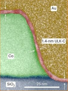
The team produced the carbon film using chemical vapour deposition, in which gases react on a surface to form a solid film. The process operated below 300 degrees Celsius and deposited the film directly on silicon dioxide, copper and cobalt. The researchers achieved uniform growth across a four-inch wafer and around the sidewalls and corners of patterned structures.
Moving towards chip manufacturing
The work builds on the team’s 2020 Nature report of stable, free-standing monolayer amorphous carbon and forms part of a wider programme supported by the National Research Foundation (NRF) Competitive Research Programme.
The team has also developed and protected intellectual property arising from the research and is now working to move the material from laboratory testing towards semiconductor manufacturing. In April 2026, NUS commenced a formal research collaboration with TSMC to evaluate the material for ultralow-k insulation and chipmaking. Three months later, the team began a National Research Foundation Central Gap Fund project to scale its low-temperature, ultraviolet-assisted deposition process and address integration, reliability and manufacturability.
“Our next task is to translate this performance to industry-relevant wafers and determine how the film can be incorporated into existing chipmaking processes,” added Prof Oezyilmaz. “Through the Central Gap Fund project and our collaboration with TSMC, we will test its long-term reliability, consistency at scale and compatibility with established manufacturing standards.”