Research Areas & Facilities
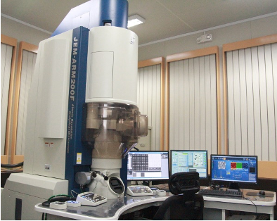
The MSE Department at NUS is specialised in Scanning Transmission Electron Microscopy (STEM): an electron beam with a diameter smaller than an atom is scanned over a material, to show its structure at atomic resolution.
Atomic-resolution elemental mapping can also be performed with our STEM, using the techniques EDS and EELS (Energy-Dispersive X-ray Spectroscopy and Electron Energy-Loss Spectroscopy). It is even possible to measure optical properties of materials, such as local band gap energy in semiconductors, and localized surface plasmon modes in noble metals.
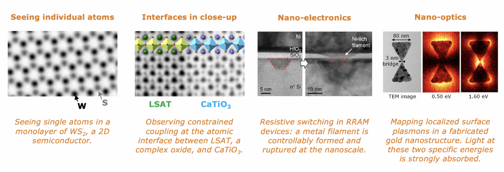
Being able to observe materials directly at atomic resolution allows us to measure new materials properties at surfaces and interfaces. For example: individual dopants and vacancies in 2D materials can be imaged. It is also possible to study microelectronic logic- or memory devices at the ultimate resolution, with the help of careful, site-specific sample preparation.
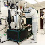
 CA2DM CA2DMThe Centre for Advanced 2D Materials directed by Prof. Antonio H. Castro Neto was formed in 2014 when the National Research Foundation (NRF) of Singapore has awarded NUS with a S$ 50 M grant over the next 10 years in order to support the operational costs of CA2DM’s labs and micro and nano-fabrication facility. It focuses on the exploration, synthesis, and development of new devices based on two-dimensional (2D) materials of which graphene is the most famous. |
|
NUS T11 Shared Facilities houses state-of-the-art equipment in all its respective laboratories and affiliated research institutes enabling researchers, staff and students to carry out cutting edge research activities. NUS T11 Shared Facilities creates an environment which facilitates an open sharing environment for building outstanding research teams and access to top-end research facilities. |
|
The Applied Materials-NUS Advanced Materials Corporate Lab combines Applied Materials’ leading expertise in materials engineering and semiconductor technologies with NUS’ world-class and multi-disciplinary R&D capabilities that span applied chemistry, materials science and microelectronics process engineering. The collaboration will focus on R&D in advanced materials engineering with the intent to create innovations that can be quickly transferred into commercial applications. |
|
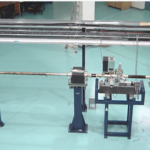
The Singapore Synchrotron Light Source, SSLS,is a University-level Research Centre at the National University of Singapore, under the office of the Deputy President (Research & Technology), with activities involving local and international groups from many universities, research institutes, and industry.It currently has a R&D programme featuring micro/nanofabrication, a variety of analytical applications, and the development of advanced synchrotron radiation instrumentation. |
|
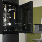
The CBIS Cryoelectron Microscope Facility is a prominent member of a select group of state-of-the-art, high-end cryoelectron microscopy facilities in the world. By minimizing EMI, reducing relative humidity to 30%, and together with the exceptionally quiet acoustic and low mechanical vibration levels, all microscopes in the facility are able to easily reach designed performance specifications. |
| Date | Title | Speaker |
|---|---|---|
| 07 December | Additive Manufacturing of Functional Ceramics Structures in the Fields of Water Treatment |
Mr. Win Jonhson |
| 22 September | Magnetic Immunity and Thermal Stability Assessment of STT-MRAM Devices |
Mr. K Sivabalan |
| 15 September | Toughening of Biodegradable Polymers by Entropic Mixing: Towards Sustainable Plastics |
Mr. Hou Xunan |
| 16 August | Developing Super-Hygroscopic Materials for Multifaceted Applications |
Ms. Yang Jiachen |
| 19 July | USING PHOTOSYNTHETIC PROTEINS FOR ENERGY STORAGE AND SENSORY DEVICES |
Ms. Nikita Paul |
| 5 July | TOWARDS LONGER WAVELENGTH III-NITRIDE LEDs THROUGH CONCERTED USE OF ELECTRON MICROSCOPY AND COMPUTATIONAL MODELING | Mr. Tara Prasad Mishra |
| 27 Jan | Nickel-based Catalysts for High Performance Ammonia Electrooxidation |
Ms. Zhu Mingke |
| 5 Jan | CURRENT-INDUCED MAGNETIC FIELD-FREE SWITCHING OF PERPENDICULAR MAGNETIZATION |
