



Researchers at CDE have identified a key design principle for building reliable electronics from materials only one atomic layer thick, giving engineers a clearer way to control unwanted electrical leakage in future ultra-small devices.
The finding challenges the assumption that material choice alone determines device performance.
“At this extremely small scale, we’ve shown that tiny physical gaps between electrodes can matter more than the material’s own ability to block electrical current,” said Professor Mario Lanza, from the Department of Materials Science and Engineering and the NUS Institute for Functional Intelligent Materials, who led the study.
“To design reliable advanced chips, memory technologies and other next-generation components, we need to look at the whole structure, including how the material sits between its electrodes and the actual distance electrons have to cross.”
The researchers’ findings could help guide the development of future electronic components that are smaller, thinner and more energy-efficient. These include advanced computer chips, ultra-thin memory devices, and emerging technologies that rely on controlling electrical behaviour at the atomic scale.
The study was published in Nature Materials on 1 July 2026.
“So-called 2D materials open up the possibility of building electronic devices far thinner than is possible with conventional materials,” Prof Lanza said. “But when a material becomes extremely thin, electricity can behave in unexpected ways. At this scale, electrons can slip through barriers that are meant to stop them - a process known as quantum tunnelling- creating unwanted leakage current that can affect how well a device works.”
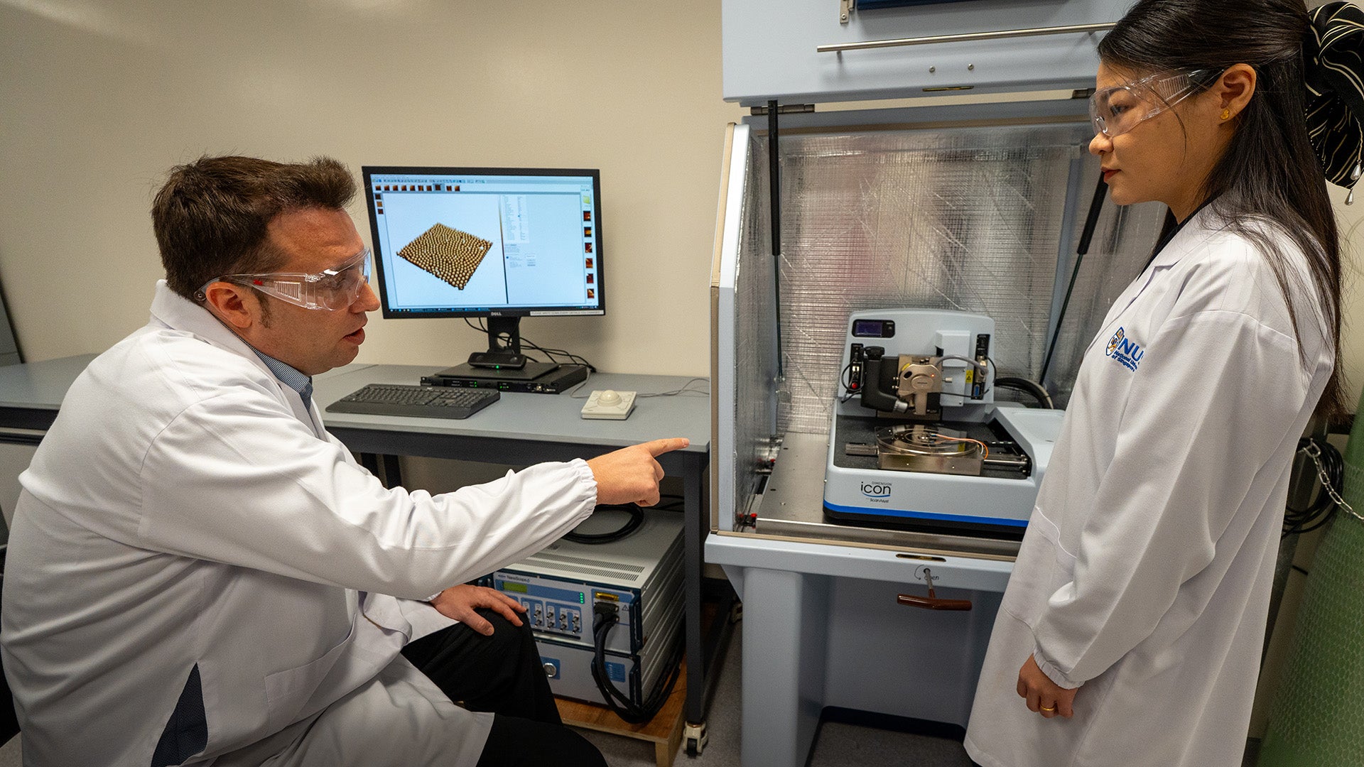
The NUS-led team found that this leakage is strongly influenced by how the device is assembled.
If an atom-thin material is placed on a slightly uneven metal surface, tiny gaps can form between the material and the electrode. These gaps change the distance that electrons must cross, which can greatly alter how much current leaks through.
" When the material is less than one nanometre thick, even a very small change in physical distance can have a major effect on how easily electrons pass through "
This discovery helps explain why previous experiments on similar materials sometimes produced very different results. Devices that looked similar may, in fact, have had tiny gaps at their interfaces, leading to very different electrode-to-electrode distance, and therefore causing different electrical behaviour.
“One of the surprising lessons from this work is that conventional expectations about insulating materials can change at the atomic scale,” said Dr Yue Yuan, first author of the study. “When the material is less than one nanometre thick, even a very small change in physical distance can have a major effect on how easily electrons pass through.”
The team studied several atomically thin materials, including hexagonal boron nitride, molybdenum disulphide and tungsten disulphide.
“Although hexagonal boron nitride is generally expected to be a strong insulator, we found that in monolayer form it actually allowed more current to pass through than some materials with weaker insulating properties such as molybdenum disulphide and tungsten disulphide,” said Dr Yuan. “This is because the monolayer of hexagonal boron nitride is physically much thinner, giving electrons a shorter distance to tunnel.”
The researchers combined nanoscale electrical measurements, device-level testing and computational modelling to understand how structure affects leakage. They compared devices with atomically flat graphite electrodes to those with rougher metal electrodes, such as gold and ruthenium. The results showed that rougher electrodes can lead to lower, more variable leakage currents due to the tiny gaps they create.
The findings show that engineers should not assess atom-thin materials solely by their intrinsic properties, such as their resistance to current flow. Instead, they need to consider the full device structure, including electrode roughness, interface quality, tiny voids, contaminants and the true distance between electrodes.
“This study provides a foundation for designing more reliable atomically thin electronic devices by improving interface uniformity, engineering smoother electrodes and minimising nanoscale gaps and contaminants,” said Prof Lanza.
The research was conducted in collaboration with partners from KAUST, TU Wien, the University of Modena and Reggio Emilia, the University of Granada, RWTH Aachen University, AMO GmbH and The University of Texas at Austin.