- Deposition and Growth
- Annealing Process
- Magnetic Processing
- Lithography
- Etching
- BEOL and Packaging
- Characterisation and Metrology
- Atomic Force/Scanning Probe Microscopy (AFM/SPM) – Park NX20
- Ellipsometer – Semilab SE-2000
- Field Emission Scanning Electron Microscope (FE-SEM) – Hitachi Regulus 8100
- Field Emission Scanning Electron Microscope (FE-SEM) – Hitachi Regulus 8230
- Focused Ion Beam Scanning Electron Microscope (FIB-SEM) – Tescan GAIA3
- Raman Microscope – Renishaw inVia
- Scanning Magneto-Optical Kerr Effect (SMOKE) Microscope – Evico Magnetics
- Surface Profiler – Bruker DektakXT
- Superconducting Quantum Interfernce Device (SQUID) Magnetometer – Quantum Design MPMS3
- Vibrating Sample Magnetometer (VSM) – MicroSense EZ9
- X-ray Diffractometer (XRD) – Rigaku SmartLab
- Others
- Tool Booking
ETCHING
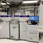
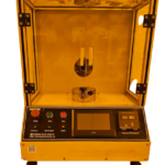
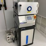
Etching is a process for pattern transfer and surface treatment in micro-nano device fabrication. E6NanoFab makes available dry and wet etching systems to support the diverse process requirement.
Dry Etching
Multi-chamber cluster tools such as ICP plasma etching and ion beam milling provide strong dry etching capabilities for various materials such as Si, III-V & III-N, oxides, metals, polymers and others.
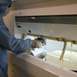
Wet Etching
Our dedicated wet-benches support several wet processes such as RCA, standard cleaning, and orientation dependent Si KOH etching.