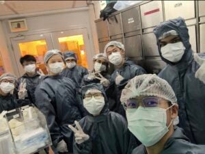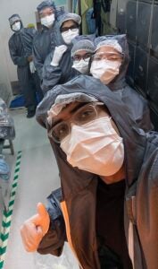
A key highlight of the initiative was on-site visits to semiconductor research and fabrication facilities, where students observed the end-to-end chip development pipeline. This included exposure to major stages such as device design, wafer fabrication, lithography, deposition, etching, testing, and packaging. Seeing these processes firsthand helped students understand the complexity, precision, and interdisciplinary coordination involved in modern chip manufacturing.
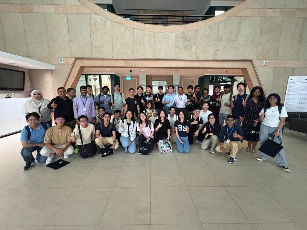
Overall, the initiative bridged theory and practice by connecting coursework to real semiconductor workflows, research infrastructure, and career pathways in advanced electronics and industry R&D.