Discovery breaks resolution limitations in microscopy; Potential applications in high precision failure inspection and biological research

The optical microscope is a critical equipment for scientific research and failure inspection in high precision industries. However, for centuries, the imaging resolution of microscopes is fundamentally limited by the diffraction limit of light. Existing efforts to break this fundamental diffraction limit through various technologies suffer from limitations such as a near-field operation, which requires the sample to be close to the microscope, or the dyeing of samples, which is an invasive process that affects the quality of the sample.
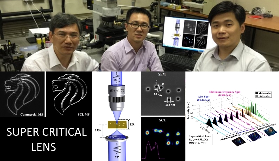
A research team led by Professor Hong Minghui and Associate Professor Qiu Cheng Wei from the Department of Electrical and Computer Engineering at NUS Faculty of Engineering has developed a novel supercritical lens, which enable optical microscopes to capture images in real-time and with greater detail beyond diffraction limit. In addition, this technique does not require any pre-treatment of samples or post-processing of the image.
Prof Hong said, “Our breakthrough is achieved in a totally non-invasive manner, coupled with the capability of real-time imaging. This could potentially open up a wide range of applications in areas such as high precision failure inspection in the semiconductor industry, and will also contribute significantly to biological research.”
High-performance, ultra-thin lens that is easy to fabricate at low cost
Planar metalens is a high-performance, ultra-thin lens which has extraordinary capabilities in light modulation, as compared to traditional three-dimensional bulky optical lens. The NUS team’s supercritical lens, which is based on the concept of an optimised planar metalens, is developed using a new algorithm and it can be easily fabricated by a commercial laser pattern generator in high speed and at low cost.
Specifically, the team demonstrated an imaging resolution of 65 nanometres using the supercritical lens microscope, as compared to typical microscopes which have an imaging resolution of around 120 to 150 nanometres. In addition, this novel microscopy technique exhibits a significantly longer working distance of 55 micrometres, thus providing additional space for easier handling and adjustment of samples in real-world applications, and allowing the samples to be observed in greater detail.
Assoc Prof Qiu added, “Using a lens with microscale feature size, we have achieved nanoscale imaging resolution. Our invention could potentially bridge the wide gap between laboratory proof-of-concept demonstrations and practical applications for the super-resolution imaging technique.”
Wide-ranging applications
This discovery by NUS researchers holds great promise for nano-imaging of semiconductor devices, and could enable faster, cost-effective and more accurate detection of defects in components such as integrated circuit chips which require imaging resolution that is less than 100 nanometres (sub-diffraction resolution). Current methods of defect detection require the use of the scanning electron microscope, which is a specialised and expensive equipment, and the process also needs to be operated in a vacuum environment.
In the area of biological research, most protein and cellular tissues require sub-diffraction limit imaging, thus resulting in the need for the dyeing of samples. The team’s invention could potentially lead to non-invasive investigation of the interior of biological cells, thus allowing researchers to study samples at a much deeper level than ever before. And this may eventually contribute towards new medical discoveries.
The findings of the study were published in the scientific journal, Advanced Materials, in February 2017.
Moving forward, the NUS team plans to further enhance the imaging resolution of the novel lens and explore new applications for the technique. They have also filed a patent for the technology and is exploring opportunities to work with industry partners to commercialise their invention.


