Power Electronics Laboratory
The Power Electronics Laboratory is located at Engineering Block 3, Level 2 to facilitate the teaching and research needs in the multi-disciplinary technical area of power electronics, especially in the field of wafer-level power semiconductor device characterisation, power integrated circuit design and MEMS sensor/actuators design and measurements.
Currently, the laboratory supervisor is A/Professor YC Liang (6516 2175) and the laboratory officer in charge is Ms. MC Sai (6516 6925).
The laboratory hosts PhD research students, MSc project students and final year project students. It also hosts undergraduate teaching laboratory sessions on the power semiconductor device measurement, silicon microsystem and solar photovoltaic characterisation.
Research Activities highlight on Power Microelectronics
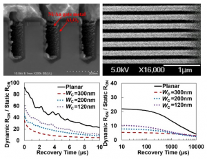 |
AlGaN/GaN Fin-gate HEMT devices are designed and fabricated, achieving 75% reduction of current collapse phenomenon, which is a critical issue of planar-gate HEMT. The fin-width is as small as 50 nm made by the e-beam lithography process. This fin-HEMT structure can extend its usage beyond a power device, as IoT sensors for GaN integrated circuits. |
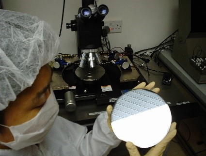 |
Power Semiconductor Wafer inspection and characterisation: Students in course EE4505 will learn how to use the probing station and HP4142B to test a pre-fabricated an IGBT and sensor wafer. Some wafer inspection on MEMS structures is also carried out with the same probing station in course EE4509. |
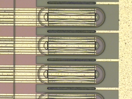 |
A microscopy photo of fabricated smart power IGBT device with in-built current sensor and protection circuits. This was done by the research student J. Luo. |
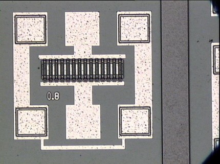 |
The microscopy photo of an RF-LDMOS fabricated on silicon wafer with partial SOI process technology applied: The said LDMOS have lower parasitic capacitance between drain and source (50% less) in order to boost up the power-added efficiency of the 2-4 GHz amplifier system. The project was funded by A*STAR and in collaboration with IME (Institute of Microelectronics, Singapore). |
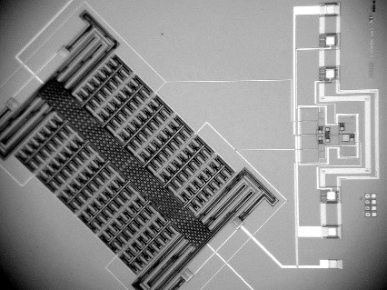 |
An integrated microgyroscope with CMOS detection circuits: The detection electronics is to use high-frequency carriers to measure the changes in comb capacitance to sense the displacement of lateral beams to identify the rate of rotation. This work was done by research students T Zhao and SS Boh. |
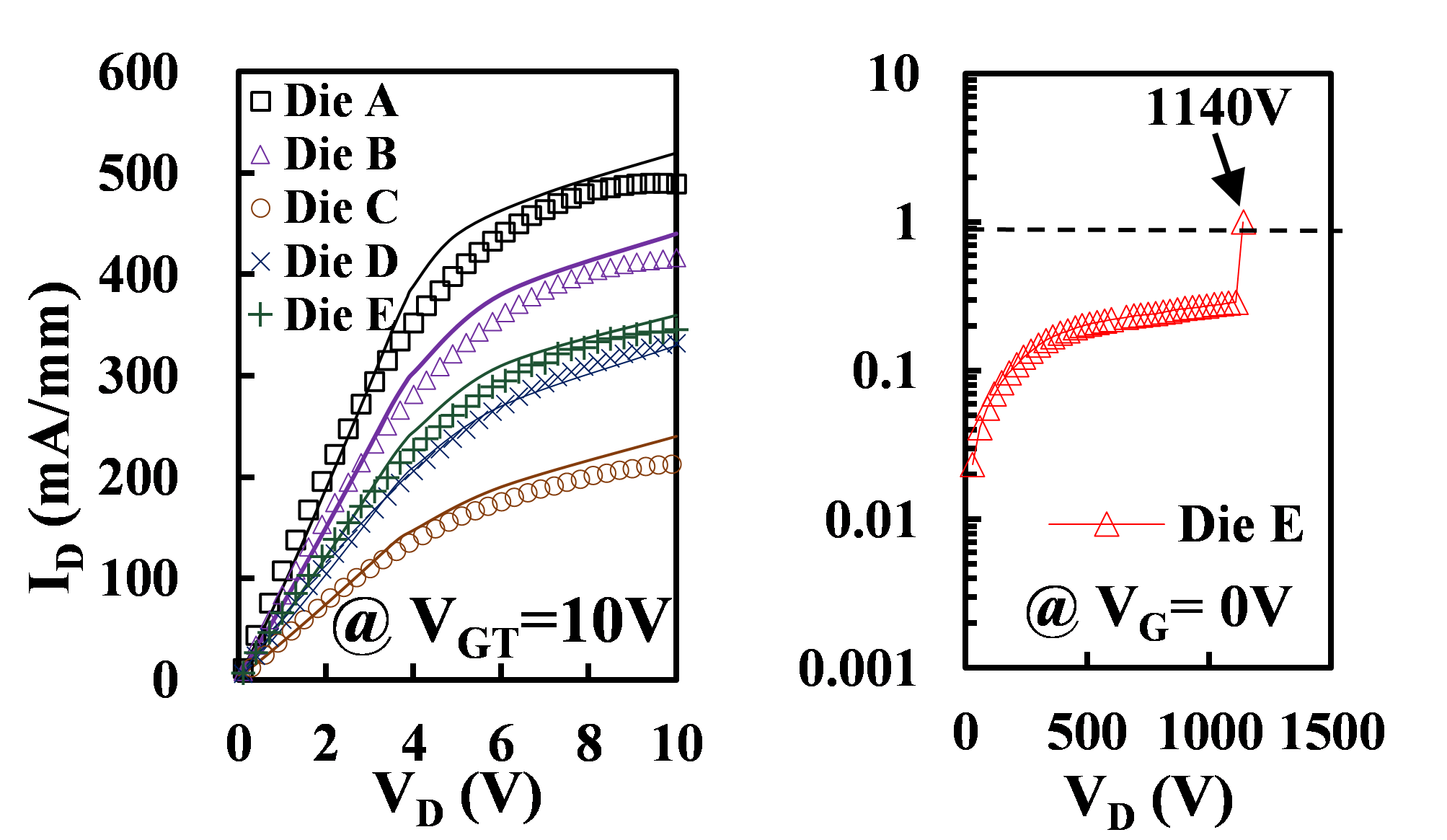 |
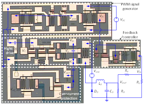
The GaN Power HEMT devices of breakdown voltage of 1140V and saturation current of up to 500 mA/mm. The research work was later extended into full-GaN power integrated circuits for DC-DC converter applications (figure as shown). The recent GaN work includes LED-HEMT power integration for IoT applications, Hall-effect sensor integration for machine condition monitoring, and PH sensor integration for the environmental monitoring. |
 |
|

